BTC $72,281.27 -1.78%
ETH $2,006.62 -2.03%
BNB $654.00 -3.94%
XRP $1.02 -2.85%
SOL $81.08 -3.50%
TRX $0.3155 -0.52%
DOGE $0.0651 -4.23%
ADA $0.1694 -4.28%
BCH $225.30 -2.39%
LINK $9.86 -4.37%
HYPE $70.05 -4.10%
AAVE $111.87 -9.29%
SUI $0.7897 -5.25%
XLM $0.1434 -4.01%
ZEC $968.91 -1.44%
AAPL $358.02 +2.71%
AMZN $270.69 -0.85%
GOOGL $293.82 +1.11%
MSFT $524.14 -2.50%
META $626.59 -3.50%
NVDA $153.35 -12.23%
TSLA $386.30 +0.16%
SNDK $892.00 -4.46%
INTC $59.47 -3.54%
SPCX $138.72 -2.64%
MU $766.09 -1.07%
AMD $562.03 +3.06%
BTC $72,281.27 -1.78%
ETH $2,006.62 -2.03%
BNB $654.00 -3.94%
XRP $1.02 -2.85%
SOL $81.08 -3.50%
TRX $0.3155 -0.52%
DOGE $0.0651 -4.23%
ADA $0.1694 -4.28%
BCH $225.30 -2.39%
LINK $9.86 -4.37%
HYPE $70.05 -4.10%
AAVE $111.87 -9.29%
SUI $0.7897 -5.25%
XLM $0.1434 -4.01%
ZEC $968.91 -1.44%
AAPL $358.02 +2.71%
AMZN $270.69 -0.85%
GOOGL $293.82 +1.11%
MSFT $524.14 -2.50%
META $626.59 -3.50%
NVDA $153.35 -12.23%
TSLA $386.30 +0.16%
SNDK $892.00 -4.46%
INTC $59.47 -3.54%
SPCX $138.72 -2.64%
MU $766.09 -1.07%
AMD $562.03 +3.06%

wafer

All
Article
Flash

first_img Samsung Electronics executive: It is expected that HBM will account for nearly 30% of DRAM wafer production capacity next year

According to a report by the Financial Associated Press citing local media on September 29, Samsung Electronics Executive Vice President Kim Taewoo stated that HBM is expected to account for nearly 30% of the total wafer capacity of DRAM manufacturers next year, up from the current ratio of about 20%. He mentioned that HBM competes with traditional DRAM for the same batch of wafer capacity, and increasing HBM output may squeeze the supply of traditional DRAM.TrendForce previously predicted that by the end of 2027, the HBM wafer input from the three major global HBM suppliers will account for about 30% of the total DRAM wafer input, but in terms of storage capacity, it will only contribute about 13% of the total DRAM supply. Additionally, according to media reports on September 20, Samsung began mass production and shipment of HBM4 in February this year and provided 12-layer HBM4E samples to customers including NVIDIA in May; the industry expects Samsung's monthly wafer input for HBM to increase from about 180,000 wafers this year to about 250,000 wafers next year.On the same day, TrendForce stated that the demand for AI servers continues, and HBM and general DRAM will still share limited advanced process capacity. The storage supply will remain tight in 2027, and the price expectations for HBM in 2027 have been raised, with an expected year-on-year increase of 121% in the mixed average selling price. Due to limited supply and rising system costs, 8-layer HBM is expected to become a priority evaluation option for several manufacturers in 2027, with its price per Gb expected to be about 10% to 20% higher than that of 12-layer products.

first_img Major manufacturers increase orders, TSMC's 2-nanometer monthly production capacity is expected to reach 120,000 wafers by the end of the year

According to the Economic Daily, major companies such as Apple, NVIDIA, AMD, Qualcomm, and MediaTek are racing towards AI and high-performance computing, recently increasing their orders for TSMC's 2-nanometer family capacity by 10% to 20%. As a result, TSMC is accelerating the expansion of its 2-nanometer family, with progress exceeding expectations. TSMC has consistently refrained from commenting on customer information and market rumors.The market originally estimated that TSMC's monthly capacity for the 2-nanometer family would be around 90,000 to 100,000 wafers by the end of this year, with expectations for continued double-digit growth to reach 110,000 to 140,000 wafers by 2027. Industry sources indicate that due to strong customer demand, the monthly capacity is expected to surge to 120,000 wafers by the end of this year, achieving the originally set 2027 target ahead of schedule. Sources say that in response to the demands from Apple and non-Apple customers, the speed and scale of new capacity for the 2-nanometer family are setting new records, far exceeding the ramp-up speed of the 3-nanometer family in its first year.TSMC's Senior Vice President and Co-COO, Wei Chen-Hao, stated at this year's North America Technology Forum that in response to strong demand from AI and other sectors, there will be five 2-nanometer fabs ramping up simultaneously for the first time this year, including two in Hsinchu and three in Kaohsiung; the wafer output in the first year of 2-nanometer will increase by 45% compared to the first year of 3-nanometer in 2023; the compound annual growth rate of 2-nanometer capacity from 2026 to 2028 will reach 70%. TSMC's 3-nanometer capacity in the Southern Taiwan Science Park is expected to reach nearly 180,000 wafers per month in the fourth quarter of this year, and three new 3-nanometer fabs are being established in Taiwan, Arizona in the United States, and Japan. The second fab in the United States is planned to begin mass production in the second half of 2027.

first_img The supply chain states that TSMC will increase wafer prices by 3% to 6% starting from January 2027

Supply chain sources say that TSMC's wafer foundry prices are set to rise again, with adjustments to Wafer Out prices based on different processes starting from January 2027, with an increase of about 3% to 6%. The utilization rate of 8-inch factories exceeds 100%, and processes below 45 nanometers are fully loaded, with order visibility extending to 2030. The increase for advanced processes is higher, while mature and specialty processes are negotiated individually based on products, utilization rates, and customer conditions. TSMC has not responded to market rumors.Supply chain sources indicate that TSMC's 2-nanometer and 3-nanometer processes are in short supply, and the pressure on advanced packaging capacities such as CoWoS has not been alleviated. Customers find it difficult to switch suppliers immediately even in the face of price increases. The factory in Arizona, USA, reflects higher manufacturing costs, and the foundry quotes remain high. After the price adjustment, quotes from foundries such as Samsung Electronics, Intel, United Microelectronics Corporation, and World Advanced, as well as testing and packaging factories and IC design customers, may also be affected. United Microelectronics Corporation, Powerchip Semiconductor Manufacturing Corporation, and World Advanced have announced price increase strategies, which will continue until 2027.The supply chain states that this wave of AI demand has increased the need for PMIC, MCU, driver ICs, analog ICs, and sensors, in addition to GPUs, ASICs, and HBM. IC design companies point out that after the wafer price increase, product costs need to be reassessed, with higher-end GPUs and ASICs having relatively larger pass-through space. TSMC Chairman Wei Zhejia has stated that customers do not switch wafer foundry partners just because they are dissatisfied today. Supply chain sources say that orders transferred from Google, Apple, NVIDIA, and others mostly involve non-core chips or limited-scale orders, with no significant changes observed in the high-end process customers' chip placements.

first_img The supply-demand gap for silicon wafers will expand from about 8% by the end of 2026 to 24% by 2028

According to the Industrial and Commercial Times, with the expansion of HBM and advanced logic below 2 nanometers, it is estimated that the global silicon wafer supply-demand gap will widen from about 8% by the end of 2026 to 15% in 2027 and 24% in 2028. GlobalWafers, Siltronic, and TSMC are expected to benefit from this. It is noted that mid-2027 will be a critical turning point; if the pace of supply expansion does not keep up, a new wave of shortages and rush buying may occur from the second half of 2027 to the first half of 2028.SEMI statistics show that the global silicon wafer shipment area reached 3.573 billion square inches in the second quarter of 2026, an increase of 9.1% quarter-on-quarter and 7.4% year-on-year. It is estimated that the global monthly production capacity of 12-inch silicon wafers will be about 10.69 million pieces in 2026, an increase of 7% year-on-year, with only about a 3% increase to 11 million pieces in 2027, and an increase of about 6% to 11.7 million to 11.76 million pieces in 2028. The new supply includes about 300,000 pieces from the second phase of GlobalWafers and about 100,000 pieces from Siltronic.It is estimated that the consumption of HBM silicon wafers will increase by 23% and 28% in 2027 and 2028, respectively; new general DRAM production capacity will gradually come online starting in 2027, with an additional monthly capacity of about 350,000 to 450,000 pieces by 2028. In terms of advanced logic, the consumption of logic process silicon wafers is expected to increase by 12% and 11% in 2027 and 2028, respectively. Currently, customer silicon wafer inventory remains at about 100 to 120 days, and it will take time to digest to the normal level of 50 to 70 days.

first_img Micron plans to expand HBM production capacity to approximately 100,000 wafers per month by the end of the year

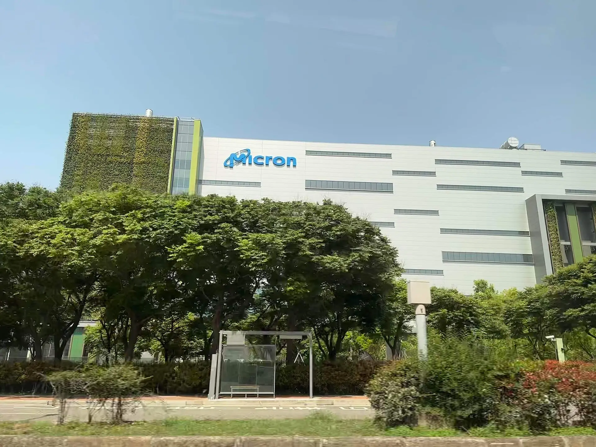
According to Electronic News on September 3, Micron plans to double its high bandwidth memory (HBM) production capacity compared to last year, with a maximum addition of 60,000 wafers per month by the end of this year. Insiders say that Micron's HBM output was about 40,000 to 50,000 wafers per month last year, and it is expected to reach about 100,000 wafers per month by the end of the year, narrowing the gap with Samsung Electronics and SK Hynix.Micron is increasing procurement orders from multiple HBM equipment suppliers, with production bases mainly in Taiwan and Singapore, continuously introducing equipment. Currently, the output is mainly HBM3E 12-layer, with HBM4 12-layer accounting for about 20% to 30% at the beginning of this year, which may rise to as high as 50% by the end of the year. HBM4 12-layer will be used in NVIDIA's latest AI accelerator, Vera Rubin, and Micron has started mass production of this product since the second quarter of this year.Micron CEO Mehrotra stated in the Q3 earnings call for fiscal year 2026 in June this year that the ramp-up speed of HBM4 12-layer mass production is about twice that of HBM3E 12-layer, and cumulative revenue from HBM4 shipments has exceeded $1 billion. The industry believes that Samsung and SK Hynix each have HBM production capacities of about 150,000 to 200,000 wafers per month. Counterpoint data shows that in Q2 of this year, the global HBM market shares were SK Hynix 50%, Samsung 32%, and Micron 18%. Micron is also preparing related investments in Hiroshima, Japan.

first_img The price of semiconductor silicon wafers has increased by about 10% for the first time in over three years, benefiting companies like GlobalWafers and other Taiwanese manufacturers

According to the Economic Daily, semiconductor silicon wafers have seen a significant price increase for the first time since the COVID-19 pandemic, covering the full range of specifications including 6-inch, 8-inch, and 12-inch, with an increase starting at 10%. Industry insiders believe this is the first price adjustment in over three years, and major Taiwanese silicon wafer suppliers such as GlobalWafers, TSMC, and Hejian are expected to see improvements in revenue and profitability.GlobalWafers stated that recent demand in some end markets has gradually improved, inventory adjustments in the supply chain are healthier than in the past, and market signals are more positive than last year, but prices still depend on the product, specifications, and customer situations. TSMC mentioned that under cost pressures and demand support, they have begun communicating price adjustments with customers, and operations in the second half of the year are expected to outperform the first half. Hejian indicated that they are actively negotiating price adjustments with customers and continuing to promote advanced packaging and related products.Industry analysis suggests that this round of price increases mainly reflects the rebound in chip demand driven by AI, with increased usage in advanced and mature processes, allowing the upstream silicon wafer industry to gradually feel the recovery. Currently, the negotiation progress varies among factories and customers, with some 12-inch polished wafers already subject to new quotes with double-digit percentage increases, and discussions for 8-inch and 6-inch products are also moving in a similar upward direction.

first_img Samsung Electronics accelerates the advancement of the second phase of the Mattel wafer factory, requiring equipment suppliers to obtain SEMI certification in advance

According to ZDNet Korea, Samsung Electronics is accelerating the expansion of its advanced wafer foundry capacity in the United States. The company plans to start the second phase of construction at the Taylor wafer plant in Texas by the end of this year, aiming for mass production by 2030, and has requested major equipment partners to obtain SEMI certification in advance for subsequent equipment import and export. SEMI certification is a standard for assessing the safety of semiconductor equipment and is usually a necessary procedure before equipment leaves the country.The Taylor wafer plant is responsible for Samsung's most advanced foundry mass production tasks. The first phase is currently undergoing equipment entry and installation, with a target to start production by the end of this year, focusing on a 2-nanometer mass production process, with Tesla seen as a core customer. Samsung stated in last month's second-quarter earnings call that to respond promptly to the growing customer demand, the second phase of Taylor will commence by the end of this year. Industry insiders say that although the specific specifications for the second phase have not yet been finalized, Samsung's foundry business has already pushed forward relevant preparations in advance.Previously, Samsung had postponed the investment in the first phase of Taylor multiple times due to insufficient customers and a sluggish market, until Tesla signed a foundry agreement worth approximately 22.76 trillion won in the third quarter of last year, which accelerated construction. The actual pace of mass production in the second phase will still depend on the expansion of supply to Tesla and the progress of new major customers. Additionally, there are reports that Samsung E&A is considering dispatching dozens of construction personnel locally.

first_img Samsung Electronics advances the expansion of the P5 factory in Pyeongtaek into a three-story wafer plant

According to the Dong-A Ilbo, Samsung Electronics plans to expand the core project of the P5 1·2 factory (Fab 5·6) in Pyeongtaek, Gyeonggi Province, from a dual-layer wafer factory to a three-layer wafer factory to respond to the global artificial intelligence semiconductor and memory supercycle and maximize production capacity. Samsung Electronics has recently submitted a plan to change the industrial park, proposing to increase the floor area ratio from 350% to a maximum of 490%. This change must be reviewed by the Gyeonggi Province governor and approved by the Ministry of Land, Infrastructure and Transport's industrial site policy review committee before it can be finalized.The Pyeongtaek P5 1·2 factory is the largest semiconductor factory in the world under a single standard, which began construction in 2022 and aims to be completed by 2030. It will produce high bandwidth memory (HBM), high-end DRAM, next-generation V-NAND, and advanced foundry products. The currently operational Pyeongtaek P4 uses a dual-layer structure with four clean rooms in a single building; if the change is approved, P5 will be configured with up to six clean rooms, and the number of clean rooms and production capacity is expected to increase by about 1.5 times. SK Hynix also plans to use a three-layer structure for all newly constructed wafer factories in the Yongin semiconductor cluster.Market research firm Counterpoint Research expects the global memory market size to increase from approximately 360 trillion won last year to 1,500 trillion won this year and 2,100 trillion won next year. In the context of increasingly difficult access to electricity, water, and land, increasing the floor area ratio to build three-layer wafer factories has become an important path to overcome the physical limitations of limited space and rely on the existing semiconductor industry ecosystem.

hot_img Samsung Electronics plans to repurpose the NRD-K R&D production line for wafer foundry use, aiming for mass production of 2nm base chips for HBM

According to South Korean media ZDNet Korea, Samsung Electronics is adjusting the original purpose of its NRD-K Line 2 at the Giheung campus from a research and development facility to a wafer foundry line, with the main target product being the 2nm base chips required for NVIDIA's HBM. This production line is expected to be operational in the second half of 2028, adopting a "Send-Fab" model, which involves receiving wafers from other mass production lines and performing specific processes.NRD-K is the most advanced composite research and development campus built by Samsung Electronics to seize future semiconductor technology, with a total investment of approximately 20 trillion won, planning for three production lines, of which the first line is scheduled to be completed by the end of 2024. This adjustment aims to proactively respond to the expansion of HBM demand driven by investments in AI infrastructure. Samsung plans to first apply the 2nm process to custom HBM and HBM5 to maintain performance advantages.Industry insiders point out that the scale of NRD-K Line 2 is relatively small, making it suitable for operation in the Send-Fab format. However, there are still about two years until the production line is operational, and the final purpose may be adjusted again based on market conditions. Samsung had previously considered using this production line for DRAM production, but after modifications to the relevant plans this month, DRAM capacity will be more concentrated in the Pyeongtaek campus. Equipment procurement orders have not yet been officially issued.

hot_img Silicon wafer supply tightens: 12-inch capacity is nearing full load, GlobalWafers signs a 10-year contract with Micron

According to the South Korean media The Elec, GlobalWafers stated during the Q2 earnings call that the production lines for 12-inch, 8-inch, and 6-inch wafers are nearing full capacity, with some advanced 12-inch products experiencing supply constraints due to a surge in demand for AI chips, HBM, and advanced packaging. Shin-Etsu Chemical achieved double-digit growth in 12-inch shipments both year-on-year and quarter-on-quarter in Q2, and Sungrow also believes that customer inventory adjustments are nearing completion. Although SK Siltron is gradually releasing capacity from new production lines, it is still difficult to meet the growth rate of orders.Tight supply is driving changes in long-term contract models, and GlobalWafers signed a 10-year LTA (including advance payment) with Micron last month. Prices in the non-LTA market have begun to rise and are expected to continue to increase in the second half of the year. GlobalWafers stated that it is negotiating with customers to incorporate price adjustment mechanisms into new contracts, and Nexchip also emphasized the need for "broad and meaningful price increases" to support reinvestment. Industry insiders expect that as new factories from Samsung, SK Hynix, and Micron come online, wafer demand will double in the second half of 2027, and supply shortages may further intensify.

Changxin Memory is considering building a second DRAM wafer factory in Beijing and is in talks for financing support

According to Reuters, informed sources say that Changxin Storage is considering building a second 12-inch DRAM wafer fab in Beijing's Yizhuang and is negotiating financing with the Beijing Economic and Technological Development Zone and several state-owned technology companies. The company is seeking at least 60 million yuan (approximately 8.9 million USD) in support, but negotiations are still in the early stages, and the scale and structure of the financing may be adjusted.The proposed factory will be located at the site of Changxin Storage's existing DRAM wafer fab in Beijing. The planned production capacity and total investment for the project have not yet been determined, while building a fab capable of producing advanced DRAM typically requires over 10 billion USD. Currently, Changxin Storage operates two 12-inch DRAM wafer fabs in Hefei and one in Beijing, each with a monthly production capacity of about 100,000 wafers. Changxin Storage is also building new factories in Shanghai and Hefei, and once the related projects are fully operational, the company's monthly production capacity could double to over 600,000 wafers.This expansion comes as demand for storage chips is driven by AI infrastructure, data centers, and consumer electronics entering an upward cycle. The company completed an 8.6 billion USD IPO last month, marking the largest fundraising for a semiconductor company listed in mainland China, and its stock price has risen by 13% since going public. Changxin Storage is currently the fourth largest DRAM manufacturer in the world, but Samsung Electronics, SK Hynix, and Micron together still account for nearly 90% of the global market share in the first quarter. Beijing and Shanghai are also providing funding and other support to Changxin Storage to gain economic and strategic benefits from its expansion.

hot_img TSMC is reportedly set to increase wafer foundry prices starting in 2027, with a maximum increase of 10%

According to a report by Nikkei Asia citing multiple informed sources, TSMC (TSM.N) plans to raise the foundry prices for advanced and mature process chips by up to 10% in 2027, in response to rising costs of materials, manufacturing equipment, and the construction of new overseas plants. TSMC has begun discussions with customers regarding the price increase, which involves 7-nanometer and more advanced processes. This segment contributed approximately 77% of TSMC's revenue in the quarter from April to June this year.Informed sources indicated that the basic price increase will range from 5% to 10%, depending on the customer and product. For new orders of high-performance computing (HPC) chips that exceed the customer's original forecast, TSMC plans to impose an additional premium of 10% to 15% on top of the basic price increase. As a result, the overall price increase for some advanced process chip orders may exceed 10%. In terms of mature processes (including 12-nanometer, 16-nanometer, 28-nanometer processes, and other traditional technologies), TSMC plans to raise prices by up to 10%, but some products will see increases below this level. The mature process business accounted for about 23% of the company's revenue in the last quarter. Informed sources stated that relevant negotiations began around June and were finalized in July, with the new prices set to take effect in early 2027.
app_icon
ChainCatcher Building the Web3 world with innovations.